Stop Tone Sucking cheaply and easily in your wah pedal!
Copyright 1999 R.G. Keen. All rights reserved.
"Tone sucking" is the commonest complaint about wah pedals. The design of the most common "Crybaby" wah and of the Vox reissues is a throwback to earlier years when true bypass was not considered to be an absolute requirement in pedal design. The input of the wah circuit is connected to the guitar signal all the time, and the loading of the wah input affects the treble of the guitar signal disproportionately, giving a deader sound even when the wah is "bypassed". For more information about how this occurs, see the article on "bypass technology" here at GEO.
There are two ways around this. One is to completely disconnect the wah board from the guitar signal when the wah pedal is bypassed by changing the Single Pole Double Throw (SPDT) bypass switch that is stock in most wahs for a Double Pole Double Throw (DPDT) footswitch. This converts the stock wah pedal to true bypass, and tone sucking is eliminated. However, there is the question of that DPDT footswitch and how it gets wired.
In many cases, you can achieve just as good an elimination of tone sucking by buffering the input of the wah pedal. A buffer consists of an active device that has a very high input impedance, 1M ohm or more, that will not load the guitar signal down and that will drive the wah input as well (or better!) than the guitar signal itself. This buffer is inserted between the existing input signal and the input of the wah circuit. With a buffer in place, the original SPDT bypass switch can be left in place, and tone sucking will be a thing of the past.
The easiest simple buffer is the JFET source follower. This is simple and cheap to hook into the existing wah board, and only one of the existing wah components has to be disturbed at all. This schematic shows the changes we will be doing. On the left is the original circuit, and on the right we have inserted the buffer. Even if your wah board is not exactly like the one in the following pictures, you should be able to locate the input resistor, +9V, and ground points on your board and be able to wire a buffer in.
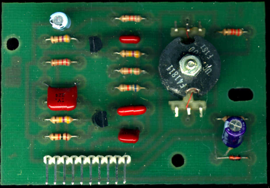
This picture shows a typical Crybaby wah board. There have been several generations of this kind of board, differing slightly in appearance, but all of which seem to share the component layout shown here. Some early ones will not have the diode we use for connections to +9V and ground, or the capacitor and resistor immediately above it. On these earlier boards, you can use your voltmeter to find a component lead that connects to +9V and ground, and transfer those connections to the alternate component leads you find. In all the cases I've looked at, the input resistor is in the same place, though. Carefully compare your wah board to this one, and only modify yours if it matches the component layout, or if you have the skills to make the modifications from the schematic if your board is differently arranged.
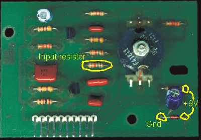
To make the mods, refer to the first steps picture. This identifies the input resistor and the points where you can tap off +9V and ground for the buffer.
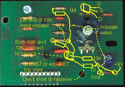
Once you have the layout firmly in mind, refer to the second mods picture. Remove the board from the case, and use a soldering iron to melt the solder on the solder side of the end of the input resistor as indicated. Use needle nosed pliers or a similar tool to avoid burned fingers and lift out the indicated end of the resistor as the solder melts. Bend the now-free end of the resistor up out of the board as indicated. Place the sharp end of a wooden toothpick or the end of a pencil near the center of the solder pad you just pulled the resistor lead from and remelt the solder so the toothpick opens up the hole and you can reinsert a new lead into it.
Take a 1M 1/4W resistor and position it as shown. Insert one of its leads under the indicated end of the resistor and solder it to the resistor lead. This connects it to ground. Slip a bit of insulation stripped from some hookup wire over the free end of the resistor and insert it into the hole vacated by the free end of the input resistor. Solder this lead on the solder side of the board and clip any excess off.
Spread the gate and drain leads of your JFET sideways away from the center source lead of the device (note - if you use a different type number JFET, you may have a different pinout, and you'll have to figure out which lead is which to connect them up). It's not a bad idea to slip bits of insulation stripped from hookup wire over the JFET leads as we will be using them for point to point wireing. Bend the end of the gate lead into a little hook, hook it under the end of the 1M resistor on the top/component side of the board and solder it in place. The JFET now sits in midair, held up by its gate lead. Bend the free end of the input resistor towards the JFET, bend a hook in the end of the center (source) lead, then bend the source lead of the JFET to the end of the resistor, hook them together and solder .
Position a 10K 1/4W resistor as shown, and clip its leads to approximate length. Form the ends into little hooks, and hook one end over the anode (non-banded) end of the diode as shown, and solder it into place. Hook the other end over the previously soldered joint between the JFET source lead and the input resistor free end, and solder it into place.
Finally take a bit of insulation and slip it over one end of the 10 ohm resistor and place the 10 ohm as indicated. The insulation will keep the leads of the 10K and the 10 ohm from shorting +9V to ground. Clip the leads to approximate length as show, form hooks on each end, and solder each end, one to +9V at the diode, and the other to the drain lead of the JFET. Note that the 10 ohm resistor is used here just as a low resistance connection, and you could simply use a piece of insulated hookup wire instead of a 10 ohm resistor.
Make sure that none of the wires short where they shouldn't, and that they go where they should. When you solder, use a well tinned tip, and use the least amount of solder you can, as any excess solder will give you misery from intermittent shorts. Also be sure that you place the 10K and 10 ohm resistors so they will not interfere with the screw that goes through the board mounting hole.
That's it! The JFET is connected to ground by the 1M resistor, and it picks up the input signal from the wiring pad that the input resistor used to connect to. The JFET drain is connected to +9V through a low resistance path. The JFET source is connected to ground by a 10K resistor, which self-biases the JFET into the linear region, and the signal is taken from the source of the JFET into the old input resistor. The input blocking capacitor that used to block the 0V signal level from the guitar from reaching the several-volt bias level of the first wah transistor now blocks the volt-or-two DC level at the JFET source from reaching the first wah transistor, so all is well from a DC bias standpoint. The JFET is happy with it's gate at ground, the guitar is happy with a 1M input resistor, and no tone sucking happens.