FXBus 1 Module 1 - a Buffer/Gain/Booster Module
Copyright 2000 R.G. Keen. All rights reserved.
 Module
1 is a little deceptive. First, it looks needlessly complex for either a buffer,
gain block, or booster. Second, for those of you who are into understanding what
circuits do by looking at schematics, it looks like it couldn't possibly do
anything useful. What are all those parts, and why are they there?
Module
1 is a little deceptive. First, it looks needlessly complex for either a buffer,
gain block, or booster. Second, for those of you who are into understanding what
circuits do by looking at schematics, it looks like it couldn't possibly do
anything useful. What are all those parts, and why are they there?
It's about options. By selectively leaving parts out and using jumpers for
others, I counted 75 different circuits/functions that can be built on that
schematic before I got tired of counting. That does not even include variations
that only have slightly different values of parts. In fact, there are doggone
few single transistor gain or buffer stages that *can't* be built on Module 1's
PCB.
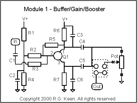
Q1 is shown as a circle with legs, no designations on the legs because it can
be a bipolar junction transistor, JFET, or MOSFET, and either NPN, PNP, P
channel or N channel. Proper choice of the other parts will make any of those
transistors work in there. For NPN and N-channel FETs, the drain is pin 1, the
base/gate is pin 2, and the emitter/source is pin3. For PNP and P-channel FETS,
pin 1 is source, pin 3 is drain.
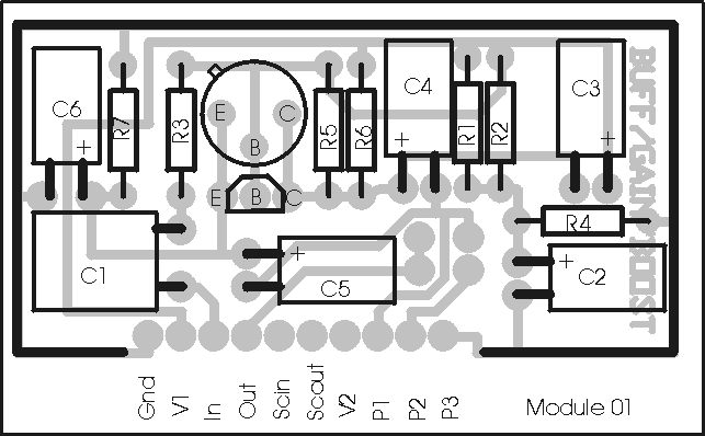
Here's how it's laid out:
Here are a few examples of what you can make this thing do:
(If a square is blank, that part is not used; a "0"
resistor is a jumper wire.)
| Circuit |
Q1 |
C1 |
C2 |
C3 |
C4 |
C5 |
C6 |
R1 |
R2 |
R3 |
R4 |
R5 |
R6 |
R7 |
Pot |
| Emitter Follower |
2N5088 |
0.1uF |
1uF |
|
|
1uF |
|
10K |
100K |
0 |
10K |
|
0 |
10K |
|
| JFET Source Follower |
2N5457 |
0.1uF |
|
|
|
1uF |
|
|
0 |
0 |
1M |
|
0 |
10K |
|
| "Improved" JFET buffer
wider input range |
2N5457 |
0.1uF |
10uF |
|
|
1uF |
|
75K |
1M |
0 |
22K |
|
0 |
10K |
|
| JFET Follower with LED bias per Orman |
2N5457 |
0.1uF |
10uF |
|
|
1uF |
|
1.5K |
1M |
0 |
LED |
|
0 |
10K |
|
| MOSFET Src. Foll. |
BS170 |
0.1uF |
0.1uF |
|
|
1uF |
|
1M |
1M |
0 |
1M |
|
0 |
10K |
|
| Bipolar gain of 10 |
2N5088 |
0.1uF |
1uF |
|
|
1uF |
|
150K |
100K |
0 |
15K |
|
10K |
1K |
|
| MOSFET gain of 10 |
BS170 |
0.1uF |
1uF |
|
|
1uF |
|
150K |
1M |
0 |
15K |
|
10K |
1K |
|
| Bipolar high gain |
2N5088 |
0.1uF |
1uF |
|
|
1uF |
22uF |
150K |
100K |
0 |
15K |
|
10K |
1K |
|
| MOSFET high gain |
BS170 |
0.1uF |
1uF |
|
|
1uF |
22uF |
150K |
1M |
0 |
15K |
|
10K |
1K |
|
| JFET gain with "coloration" per
Orman |
2N5457 |
0.022uF |
|
|
1uF |
|
22uF |
|
0 |
0 |
1M |
|
4.7K |
LED |
|
| Big Muff Input Stage |
2N5088 |
1uF |
|
|
1uF |
|
|
|
0 |
39K |
100K |
470K
par.
470pF |
15K |
100 |
Use pot output; 100K-A series with 1K to gnd. |
| Big Muff Output Stage |
2N5088 |
0.1 |
|
|
1uF |
|
|
390K |
0 |
0 |
100K |
|
10K |
2.2K |
Use pot output; 100K-A |
| Dallas Rangemaster |
2N527A |
0.0068 |
|
22uF |
|
|
|
470K |
0 |
0 |
68K |
|
4.7K |
|
Use pot output; 10K-A; hack wire pot to R7
pad |
It's easiest to understand by separating it into input options, biasing
options, and output options.
Input options.
The input circuit consists of C1 and R3, and it interacts with the value of
R2 and either R1 in parallel with R4 or R5 in parallel with R4. C1 sets the
input low frequency rolloff point in conjunction with the rest of the
resistances. Making C1 big allows the full audio spectrum to pass into the
input, making it smaller rolls off bass. You could make a treble booster for
instance, by making C1 cause a 500 Hz to 1000 Hz rolloff of bass. Where R5 is
present (that is, a voltage feedback biasing arrangement), R3 determines the
stage gain by the opamp gain equation; gain will be close to R5/R3.
Biasing Options
R1, R2, R4, and R5 bias Q1 to get the right voltages across R6 and/or R7.
We'll consider NPN and N-Channel FET's first; the PNP and P-channel FET's are
similar, just work from the positive voltage rail instead of ground.
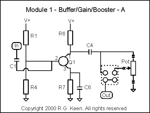
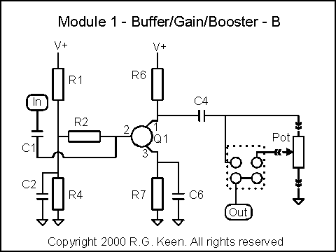
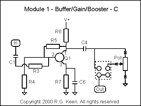
The following diagrams show the main types of biasing variation. The nominal
bias voltage set on pin 2 of Q1 (which will be the base or gate) is determined
either by the voltage divider R1/R4 (as in A and B) or by R5/R4 (C and D).
In general, either R1 or R5 but not both will be in the circuit. Sketch A shows
the standard "stabilized bias" circuit. Sketch B is the so-called
"noiseless" bias scheme, which is very similar to the usual trick of
setting up a bias voltage for opamps in effects circuits. Where a resistor in
the full-blown circuit is replaced by a wire, you simply put a cut-off resistor
lead in its position on the circuit board. Where a capacitor disappears, it's
just not populated on the board.
Sketches C and D show the two main types of voltage feedback biasing. These
have the hallmark that there is a feedback resistor from terminal 1 (collector
or drain) of the transistor. These are familiar stages from circuit sections
like the Big Muff Pi distortion.
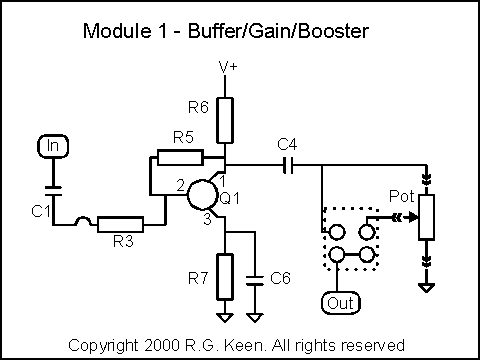
Output options
This is where we get to pick whether we get gain out of the circuit and how
much. First, we pick whether we have buffer with a gain of +1 or a gain
stage with a gain of roughly R6/R7 by choosing whether to take the output from
pin 1 through C4 (gives inverting gain) or from pin 3 through C5 (gives a
follower, or buffer). We make this selection by leaving out C4 or C5 - the pin
where there's a capacitor does the output. The "outboard" sides of C4
and C5 are tied together, and this point is also connected to to the
"hot" lug of the off-board pot. The pot allows us to have a variable
output if needed. Soldering in a wire in the four-pad block to connect the full
output (from C4/C5) or a variable output (from the wiper of the pot) selects
which it will be.
For an NPN/N-channel device, the ratio of R6 to R7 deterimines the mid
band gain. This can be modified to change the AC frequency response by selecting
values for C3, C4, C5 and C6.
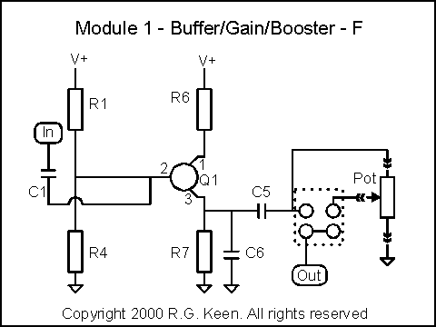
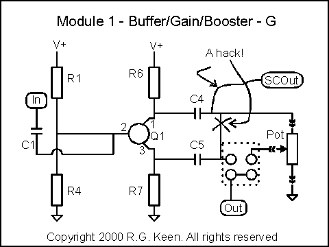
A final option is to make the module into a phase splitter as shown in
"G". We do this by
making R6 and R7 equal in value, connecting C5 as the output (gives a signal
gain of 1 to the output pin) and cutting the connection between C4 and C5. We
then use a jumper wire to connect C4 to the SCout pin, and so an inverted
version of the signal is passed to the next module on the Sidechain input. We'll
later use this one to make an octave up module set.