A DC Fault Protection Circuit for Audio Amplifiers
Copyright 2001 R.G. Keen. All rights reserved. No permission
for local copies or serving from hosts other than http://www.geofex.com.
The standard Class AB audio power amplifier allows for direct coupling of the
output of the amplifier to speakers. This is very good in that no capacitors or
transformers get in the way of the sound quality coming out. The speakers are
connected directly (more or less!) to the amplifying devices. This has the
unfortunate side effect that if an output device fails, this usually causes the
raw DC power supply to be connected to the speakers. Most speakers burn out or
are mechanically damaged by this very quickly.
Protection circuits have been designed to prevent this kind of damage, and
come in many flavors. They range from the simple - such as an added fuse in
series with the amplifier output - to the complex, with all sorts of monitoring.
The current favorite is a series relay circuit at the output of the amplifier,
driven by some sort of DC detection circuit.
Relays have their own set of problems, though, not the least of which is
reliability. Relay contacts corrode, arc and stick over time. Worse, each time
they are tested could well be the last time they operate, so there are some
built in problems. Fuses are also problematical, as they must be excruciatingly
well sized to offer good protection, and when that is done, the fuse resistance
is modulated by the heat dissipated in the fuse near maximum power, so there are
audible side effects.
Some recent advances in power MOSFETs make them attractive for replacing or
sidestepping relays and fuses on the output of the power amp. Power MOSFETs make good
switches, changing from a totally nonconductive state to a fractional-ohm
resistor in nanoseconds with the proper drive signal. Unlike bipolar transistors, there is no offset voltage
or rectification associated with a MOSFET's on-state conduction. As long as the
current through the MOSFET is low enough to not cause a significant voltage drop
across the MOSFET during current peaks, the MOSFET itself will not be
audible.
There are some difficulties with driving MOSFETs as AC relays, though. There
is an inherent substrate diode in all MOSFETs that looks to the outside world
like a diode connected across the source-to-drain. This diode conducts freely in
the reverse direction. This can actually help protect the MOSFET in some
situations, but it means that a single MOSFET can't block current in both
directions. However, putting two MOSFETs source-to-source can. The substrate
diodes then are alternately reverse biased on either signal polarity. Suitable
enhancement of gate-to-source voltage then gives us a bidirectional AC switch.
The sources are always riding on the instantaneous signal level, though, and
both gates must be made about 10-12V more positive than that moving signal
level. This is very difficult to do for most floating drive circuits.
 International Rectifier has
released several photovoltaic MOSFET drivers. These units comprise an LED to
produce light, and several photovoltaic diodes in series. When the LED shines on
the photodiodes, they produce a voltage on the output pins of the unit.
International Rectifier has
released several photovoltaic MOSFET drivers. These units comprise an LED to
produce light, and several photovoltaic diodes in series. When the LED shines on
the photodiodes, they produce a voltage on the output pins of the unit.
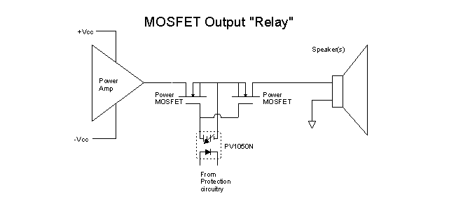
In the direct replacement for an output relay, two N-channel power MOSFETs
are connected source-to-source and gate-to-gate. The drain terminals are used as
the input and output of a switch. When the gate-source terminals of the two
MOSFETs have 0V between them, the devices are off, and no current can flow, up
to the breakdown voltage of the MOSFETs. When the gates of the MOSFETs are
several volts positive with respect to the sources, both MOSFETs are enhanced,
and current can flow. Modern MOSFETs can have a resistance from drain to source
in the milliohm region.
The photovoltaic isolator makes for a simple, easy, way to turn the two units
on or off because the voltage-source side of the isolator rides along with the
source terminals while the LED side may be tied to any level necessary for
operation. To turn the "relay" on, just force current through the LED.
To turn it off, just interrupt the LED's current.
There are people who will instinctively distrust any active solid state
device in series with an audio signal. For those people, there are two possible
alternatives: a relay to "short" the two power MOSFETs of the circuit
above and a second MOSFET protection circuit that interrupts the DC power
supply, not the speaker output. The first idea is simple - relay ills are often
caused by the wear and tear of interrupting an ongoing current. If we make the
series MOSFETs conduct just slightly before the relay contacts close and hold
for a tiny slice of time afterwards, then the MOSFETs endure all the voltage and
current stress of actually closing and opening the connection. The relay serves
only to make for a low-resistance path around any possible perturbation of the
sound by the MOSFETs.
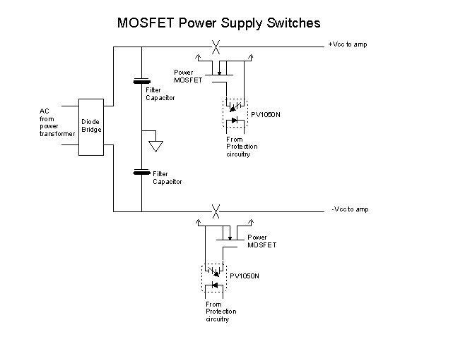 The
second version inserts the
N-channel MOSFETs into the DC power lines going from the power supply to the
amplifier itself. Each MOSFET gets its own photovoltaic isolator. When current
flows through the LEDs in the isolators, the MOSFETs are turned on, and current
flows to the amplifier.
The
second version inserts the
N-channel MOSFETs into the DC power lines going from the power supply to the
amplifier itself. Each MOSFET gets its own photovoltaic isolator. When current
flows through the LEDs in the isolators, the MOSFETs are turned on, and current
flows to the amplifier.
This version of protection is most easily thought of as a very fast relay
that can turn an amplifier's power supply off in microseconds. While the amplifier circuit
might have bypass capacitors that will still drain through the speakers, this
will be a far smaller amount of energy than the main power supply with its large
filter capacitors would feed the
speakers, and so they ought to survive in good order.
In this application, the reverse substrate diode does not matter because the
voltage is always in the correct direction to reverse bias it.
This version uses two of the photovoltaic isolators because the DC voltages
on the gate/source of the two MOSFETs are widely separated.
Another variation of this approach is to use a P-channel MOSFET in the +Vcc
line and an N-channel MOSFET in the -Vcc line, and drive both gates towards
ground with the protection circuitry for "on" and release the drive
for "off". This approach works, and suffers only in that P-channel
MOSFET devices usually have a more limited voltage and current range than
N-channel devices. They are likely to be more expensive as well.
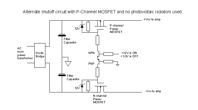
However, if you're willing to trade more expensive power MOSFETs and more
extensive drive circuitry off against the cost and availability of the
photovoltaic isolators, This circuit can work well.
The drive circuit is worth some discussion. To turn a power MOSFET fully on,
you typically need 10 to 12V of enhancement on the gate-source. However, if you
go much above this, the gate oxide can be punctured. Just to be sure that the
gate never gets outside the safe area, each MOSFET gets a 12V zener to clamp the
gate voltage to no more than 12V. The resistor parallel to the zener diode
ensures that the gate is pulled to the source voltage if there is no other drive
on it. 10K to 100K works well there.
The NPN/PNP transistor pair in the center have their collectors tied to
pull-down resistors to the MOSFET gates. These resistors are sized so that the
Vcc voltage minus 12V of gate enhancement voltage produces a reasonable current,
well within the zener's current and voltage rating. This needs to be sized
appropriately for each different Vcc level.
The PNP transistor's base is tied to ground through a resistor, and the NPN
transistor's base is the control point. Both emitters are tied together so that
whatever current the NPN transistor conducts also goes through the PNP. When the
NPN transistor's base is pulled above two diode drops, one base-emitter for each
transistor, the bases of both transistors start conducting. The two base
resistors are a safety net that ensures that the bases won't be damaged by
excessive base current. Above about 1.4V, the control pin saturates the NPN/PNP
control pair. The same control signal turns on both the NPN (in common emitter
mode) and the PNP (in common base mode), and they both pull their respective
MOSFET gates into full enhancement, and therefore full conduction.
The MOSFETs must be rated for the full voltages and currents that the power
supply can be expected to produce. For an amp with +/- 50V Vcc rails, get a
MOSFET with more than 100V, preferably more than 120V Vdsmax. Also, since
current rating is cheap in MOSFETs, get devices that ensure that there is enough
current handling capability to not "choke" the output stage of the
amp. If necessary, you may freely parallel MOSFETs to get more current
capability. Since these devices do not handle any audio (other than that audio
that is passed through the power supply) and since they are always either fully
saturated or fully off, the audio performance of the MOSFETs is really not an issue. As long as the on resistance of the MOSFET is comparable to the
source resistance of the power supply, this should be pretty transparent,
especially for modern power amps with large power supply rejection ratios.
MOSFET current rating is an issue as well. Power MOSFETs come in some
surprisingly high current ratings for the dollars you spend, and they parallel
beautifully. If you have a really high power amplifier, with maybe +/- 100V
supplies, you'll need 200V or more rated MOSFETs. You can simply parallel as
many same-type MOSFETs as you need to get a high enough current rating. They
will safely share the current they carry. An interesting point that sets MOSFETs
apart from bipolar transistors as power switches is that paralleling additional
devices does NOT require more drive current or power. All the parallel MOSFETs
you use will saturate as fully as a single one (within the limits of their
individual transconductance rating, of course). All that changes is that the
total gate-source capacitance that the voltage drive to the gate must charge and
discharge goes up as you parallel more gate-source capacitors. This means that
the transition between off to on and on to off again slow down, not that the
devices are less fully on or off. Since the transition is already so fast that
fuses look like glacial motion beside it, this isn't much of an issue. It's
likely that little or no heatsinking is needed on the MOSFETs because they
dissipate large amounts of heat only while they are actually switching - which
they don't do very often.. Simple engineering caution dictates that you don't
just assume that they dissipate no heat, but the amount is minor compared to the
output devices. The sink's thermal capacitance (that is, how long it takes to
heat up the sink itself) may be more important than the thermal resistance of
the sink because the MOSFETs normally switch only twice per session - once
on, and once off.
Devices like the IRF540 n-channel and the IRF9540 p-channel are good types to
do this with. Depending on the maker, the IRF540 is rated at up to 27 amperes
and the IRF9540 is rated at 19A. Two 9540's in the positive rail and two 540's
in the negative rail makes for a very efficient and high-current-rated
protection switch.
As to the circuitry that senses fault conditions and turns the photovoltaic isolator
LEDs on and off, there are
many ways to accomplish that, and in fact, any circuit that is a DC protector
that drives a relay can be rearranged to drive the photovoltaic isolator LEDs
as well. These circuits usually encompass a single-pole RC low pass filter with
its rolloff arranged so that the highest-level and lowest-frequency bass notes
will not cause the circuit to trip, but a DC level will cause a trip within a
few milliseconds. For any of the circuits shown here, the detector circuit
merely has to energize the LED(s) when there is no fault, and drop that current
when a fault occurs.
It's worth noting that you're not limited to DC overcurrent sense as a trip
condition. Other good conditions that can be used to activate the protection
circuit are overheated heat sinks or power transformer, sensing RF (oscillation)
on the output, and so on. With appropriate logic (CMOS works very well here)
these can help keep your amp alive.